RUV in Wafers
CRACK INSPECTION IN WAFERS
Resonance Ultrasonic Vibrations (RUV) Technology
- High reliability: 91 – 95 percent
- High throughput: 2 seconds
- Non destructive
- In-line & Off-line configurations
- UL certified
RUV TECHNOLOGY
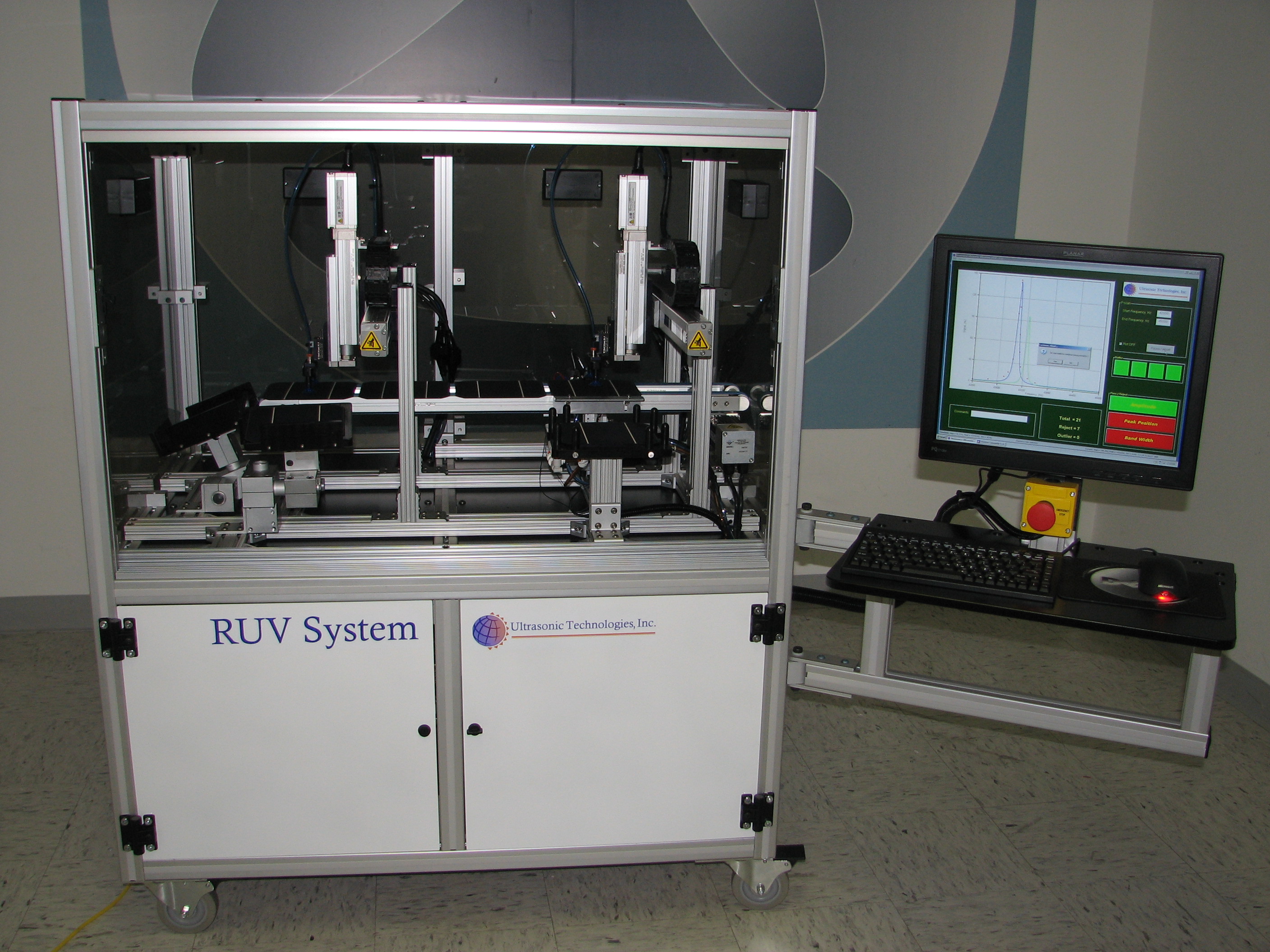
The Resonance Ultrasonic Vibrations (RUV) technique was developed for off-line and in-line non-destructive monitoring of mechanical defects (cracks, stress and delamination) in full-size bare and processed crystalline wafers including 100 microns TAIKO silicon wafers. The RUV methodology relies on a deviation of the resonance frequency response curve measured on a wafer with peripheral or bulk internal cracks in comparison with the identical defect-free wafer ultimately improving production yield. The RUV system has already proved cost savings as an in-line and QC tool in fabrication of Si solar cell, solid oxide fuel cells, ZrO2 dental ceramics, and LiTaO3 wafers for SAW application.
The RUV technology allows (1) identification of wafers with invisible mechanical defects (such as cracks and voids) at various wafer processing steps, (2) in-line characterizing voids in bonded wafers, (3) inspection wafers with build-up stress caused by ion implantation or thin-film layer deposition, and (4) screening of incoming wafers and selection of the most favorable wafer supplier.
FREQUENCY CURVE
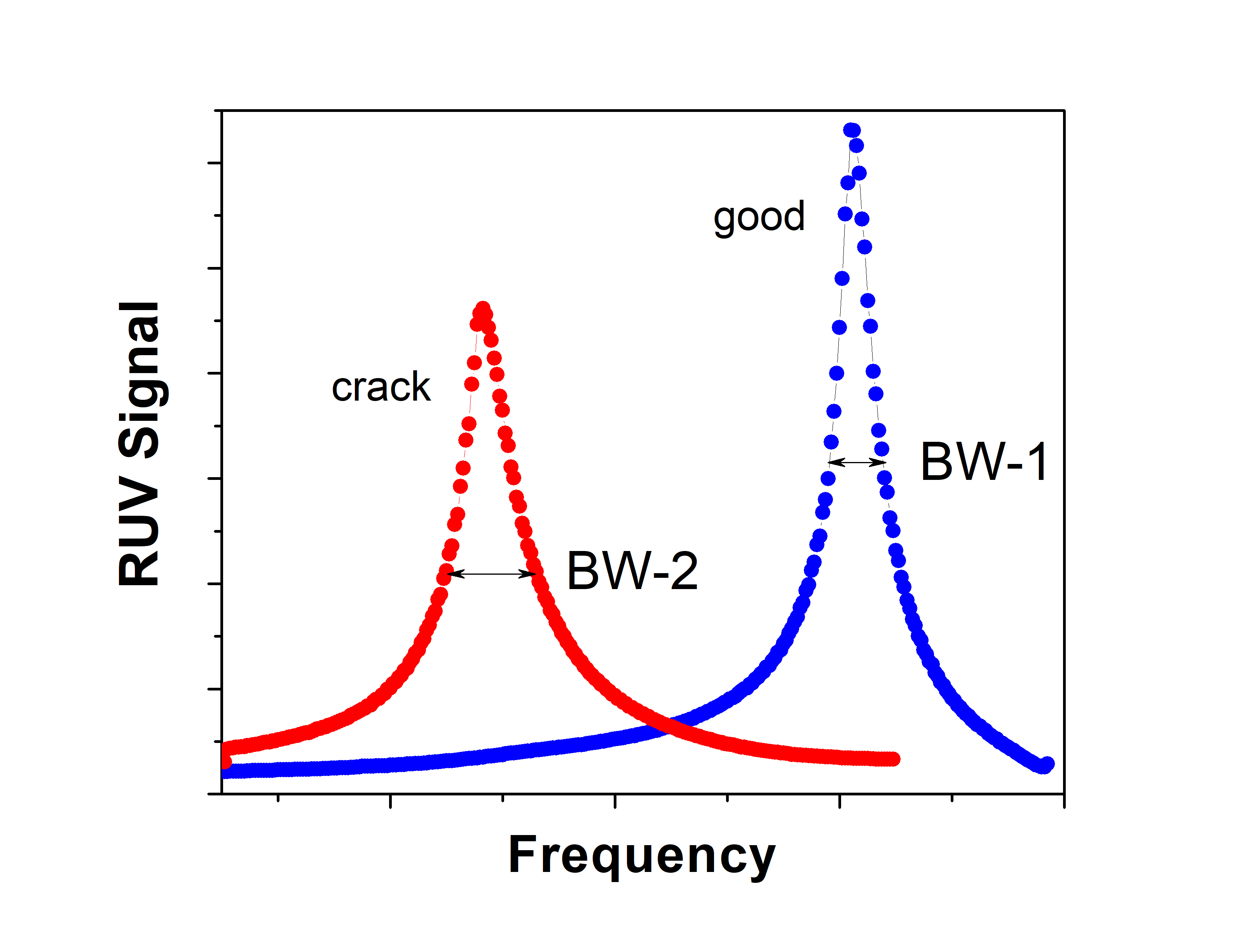
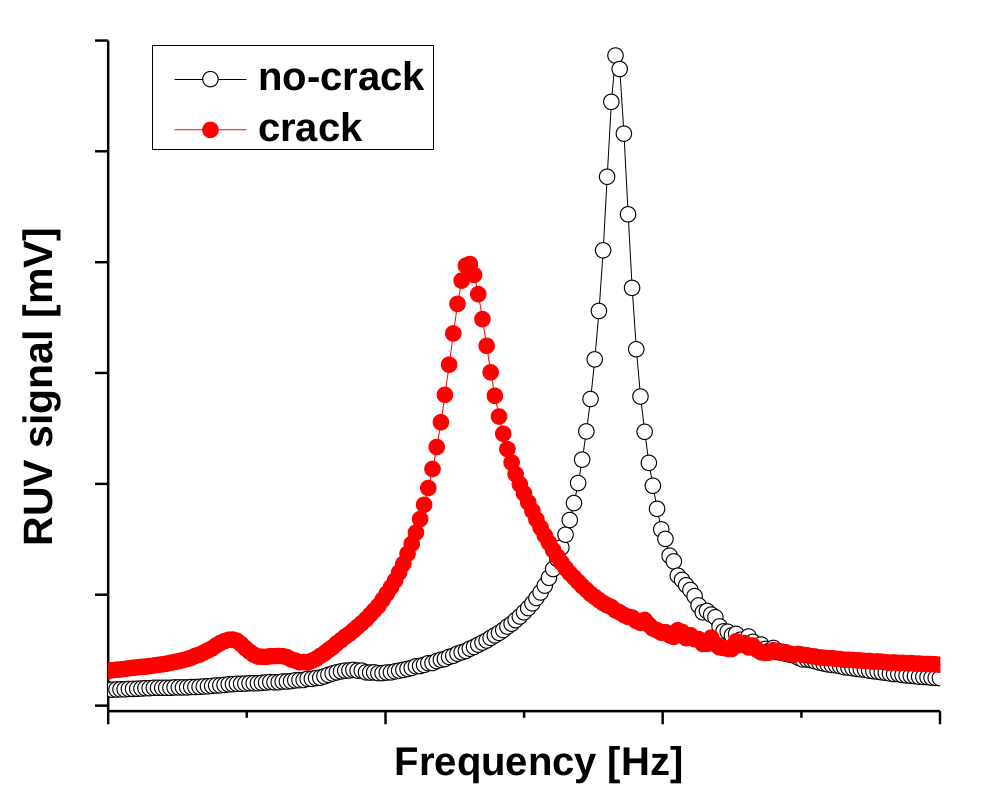
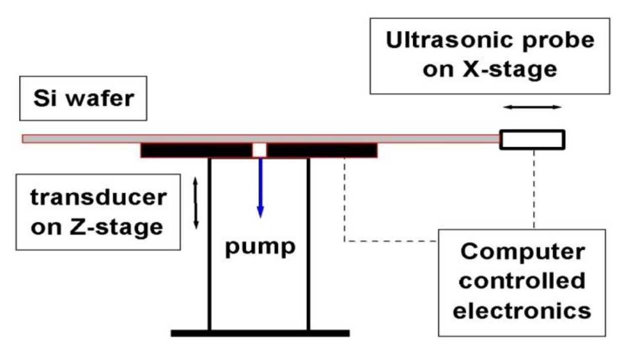
Through a resonance frequency curve selected from a broad range (20 - 250 kHz), the RUV method enables crack detection with simple criteria of inspection. A crack introduced into an ideal (non-cracked) wafer alters the RUV peak parameters: amplitude, bandwidth and peak position. Specifically, crack in the wafer shows the following features: (1) a frequency shift of the peak position; (2) an increase of the bandwidth, and (3) a reduction of the amplitude (Figure 1). Therefore, the RUV approach is based on fast measurement and analysis of a specific resonance peak and identification of the wafer if peak characteristics deviate from the normal non-cracked wafers. In Figure 2 a basic schematic of the RUV system layout is shown. A recent example is the usage of customized RUV system for 100 microns thick and 200mm diameter TAIKO wafers.
The sensitivity of the system, which refers to the length of the cracks, is adjustable to the needs of the user. The rejecting method is based on a proprietary statistical approach. In case studies the accuracy of this method was between 91 - 95%. That means that after RUV inspection the breakage caused by cracked wafers is reduced by a factor of 20. ROI of the RUV system is 6 to 12 months.
IN LINE & OFFLINE CONFIGURATIONS
Fully automatic In-line, Off-line and Quality Control RUV Tools are currently available for bare and processed wafers. For more information and a quote, please contact Ultrasonic Technologies at support page.